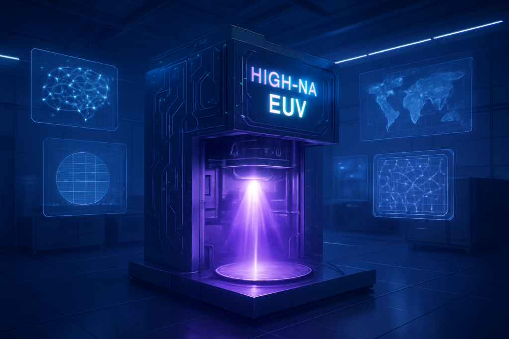
The global semiconductor landscape reached a historic inflection point in late 2025 as Intel Corporation (NASDAQ: INTC) announced the successful installation and acceptance testing of the industry's first commercial High-Numerical Aperture (High-NA) Extreme Ultraviolet (EUV) lithography tool. The machine, a $350 million ASML (NASDAQ: ASML) Twinscan EXE:5200B, represents the most advanced piece of manufacturing equipment ever created, signaling the start of the "Angstrom Era" in chip production. By securing the first of these massive systems, Intel aims to leapfrog its rivals and reclaim the crown of transistor density and power efficiency.
However, the Western technological lead is facing an unprecedented challenge from the East. Simultaneously, reports have emerged from Shenzhen, China, indicating that a domestic research consortium has validated a working EUV prototype. This breakthrough, part of a state-sponsored "Manhattan Project" for semiconductors, suggests that China is making rapid progress in bypassing US-led export bans. While the Chinese prototype is not yet ready for high-volume manufacturing, its existence marks a significant milestone in Beijing’s quest for technological sovereignty, with a stated goal of producing domestic EUV-based processors by 2028.
The Technical Frontier: 1.4nm and the High-NA Advantage
The ASML Twinscan EXE:5200B is a marvel of engineering, standing nearly two stories tall and requiring multiple Boeing 747s for transport. The defining feature of this tool is its Numerical Aperture (NA), which has been increased from the 0.33 of standard EUV machines to 0.55. This jump in NA allows for an 8nm resolution, a significant improvement over the 13.5nm limit of previous generations. For Intel, this means the ability to print features for its upcoming 14A (1.4nm) node using "single-patterning." Previously, achieving such small dimensions required "multi-patterning," a process where a single layer is printed multiple times, which increases the risk of defects and dramatically raises production costs.
Initial reactions from the semiconductor research community have been a mix of awe and cautious optimism. Dr. Aris Silzars, a veteran industry analyst, noted that the EXE:5200B’s throughput—capable of processing 175 to 200 wafers per hour—is the "holy grail" for making the 1.4nm node economically viable. The tool also boasts an overlay accuracy of 0.7 nanometers, a precision equivalent to hitting a golf ball on the moon from Earth. Experts suggest that by adopting High-NA early, Intel is effectively "de-risking" its roadmap for the next decade, while competitors like Taiwan Semiconductor Manufacturing Company (NYSE: TSM) and Samsung Electronics (KRX: 005930) have opted for a more conservative approach, extending the life of standard EUV tools through complex multi-patterning techniques.
In contrast, the Chinese prototype developed in Shenzhen utilizes a different technical path. While ASML uses Laser-Produced Plasma (LPP) to generate EUV light, the Chinese team, reportedly led by engineers from Huawei and various state-funded institutes, has successfully demonstrated a Laser-Induced Discharge Plasma (LDP) source. Though currently producing only 100W–150W of power—roughly half of what is needed for high-speed commercial production—it proves that China has solved the fundamental physics of EUV light generation. This "Manhattan Project" approach has involved a massive mobilization of talent, including former ASML and Nikon (OTC: NINNY) engineers, to reverse-engineer the complex reflective optics and light sources that were previously thought to be decades out of reach for domestic Chinese firms.
Strategic Maneuvers: The Battle for Lithography Leadership
Intel’s aggressive move to install the EXE:5200B is a clear strategic play to regain the manufacturing lead it lost over the last decade. By being the first to master High-NA, Intel (NASDAQ: INTC) provides its foundry customers with a unique value proposition: the ability to manufacture the world’s most advanced AI and mobile chips with fewer processing steps and higher yields. This development puts immense pressure on TSMC (NYSE: TSM), which has dominated the 3nm and 5nm markets. If Intel can successfully ramp up the 14A node by 2026 or 2027, it could disrupt the current foundry hierarchy and attract major clients like Apple and Nvidia that have traditionally relied on Taiwanese fabrication.
The competitive implications extend far beyond the United States and Taiwan. China's breakthrough in Shenzhen represents a direct challenge to the efficacy of the U.S. Department of Commerce's export controls. For years, the denial of EUV tools to Chinese firms like SMIC was considered a "hard ceiling" that would prevent China from progressing beyond the 7nm or 5nm nodes. The validation of a domestic EUV prototype suggests that this ceiling is cracking. If China can scale this technology, it would not only secure its own supply chain but also potentially offer a cheaper, state-subsidized alternative to the global market, disrupting the high-margin business models of Western equipment makers.
Furthermore, the emergence of the Chinese "Manhattan Project" has sparked a new arms race in lithography. Companies like Canon (NYSE: CAJ) are attempting to bypass EUV altogether with "nanoimprint" lithography, but the industry consensus remains that EUV is the only viable path for sub-2nm chips. Intel’s first-mover advantage with the EXE:5200B creates a "financial and technical moat" that may be too expensive for smaller players to cross, potentially consolidating the leading-edge market into a triopoly of Intel, TSMC, and Samsung.
Geopolitical Stakes and the Future of Moore’s Law
The simultaneous announcements from Oregon and Shenzhen highlight the intensifying "Chip War" between the U.S. and China. This is no longer just a corporate competition; it is a matter of national security and economic survival. The High-NA EUV tools are the "printing presses" of the modern era, and the nation that controls them controls the future of Artificial Intelligence, autonomous systems, and advanced weaponry. Intel's success is seen as a validation of the CHIPS Act and the U.S. strategy to reshore critical manufacturing.
However, the broader AI landscape is also at stake. As AI models grow in complexity, the demand for more transistors per square millimeter becomes insatiable. High-NA EUV is the only technology currently capable of sustaining the pace of Moore’s Law—the observation that the number of transistors on a microchip doubles about every two years. Without the precision of the EXE:5200B, the industry would likely face a "performance wall," where the energy costs of running massive AI data centers would become unsustainable.
The potential concerns surrounding this development are primarily geopolitical. If China succeeds in its 2028 goal of domestic EUV processors, it could render current sanctions obsolete and lead to a bifurcated global tech ecosystem. We are witnessing the end of a globalized semiconductor supply chain and the birth of two distinct, competing stacks: one led by the U.S. and ASML, and another led by China’s centralized "whole-of-nation" effort. This fragmentation could lead to higher costs for consumers and a slower pace of global innovation as research is increasingly siloed behind national borders.
The Road to 2028: What Lies Ahead
Looking forward, the next 24 to 36 months will be critical for both Intel and the Chinese consortium. For Intel (NASDAQ: INTC), the challenge is transitioning from "installation" to "yield." It is one thing to have a $350 million machine; it is another to produce millions of perfect chips with it. The industry will be watching closely for the first "tape-outs" of the 14A node, which will serve as the litmus test for High-NA's commercial viability. If Intel can prove that High-NA reduces the total cost of ownership per transistor, it will have successfully executed one of the greatest comebacks in industrial history.
In China, the focus will shift from the Shenzhen prototype to the more ambitious "Steady-State Micro-Bunching" (SSMB) project in Xiong'an. Unlike the standalone ASML tools, SSMB uses a particle accelerator to generate EUV light for an entire cluster of lithography machines. If this centralized light-source model works, it could fundamentally change the economics of chipmaking, allowing China to build "EUV factories" that are more scalable than anything in the West. Experts predict that while 2028 is an aggressive target for domestic EUV processors, a 2030 timeline for stable production is increasingly realistic.
The immediate challenges remain daunting. For Intel, the "reticle stitching" required by High-NA’s smaller field size presents a significant software and design hurdle. For China, the lack of a mature ecosystem for EUV photoresists and masks—the specialized chemicals and plates used in the printing process—could still stall their progress even if the light source is perfected. The race is now a marathon of engineering endurance.
Conclusion: A New Chapter in Silicon History
The installation of the ASML Twinscan EXE:5200B at Intel and the emergence of China’s EUV prototype represent the start of a new chapter in silicon history. We have officially moved beyond the era where 0.33 NA lithography was the pinnacle of human achievement. The "High-NA Era" promises to push computing power to levels previously thought impossible, enabling the next generation of AI breakthroughs that will define the late 2020s and beyond.
As we move into 2026, the significance of these developments cannot be overstated. Intel has reclaimed a seat at the head of the technical table, but China has proven that it will not be easily sidelined. The "Manhattan Project" for chips is no longer a theoretical threat; it is a functional reality that is beginning to produce results. The long-term impact will be a world where the most advanced technology is both a tool for incredible progress and a primary instrument of geopolitical power.
In the coming weeks and months, industry watchers should look for announcements regarding Intel's first 14A test chips and any further technical disclosures from the Shenzhen research group. The battle for the 1.4nm node has begun, and the stakes have never been higher.
This content is intended for informational purposes only and represents analysis of current AI developments.
TokenRing AI delivers enterprise-grade solutions for multi-agent AI workflow orchestration, AI-powered development tools, and seamless remote collaboration platforms.
For more information, visit https://www.tokenring.ai/.