In a move that signals the intensifying arms race for artificial intelligence hardware, SK Hynix (KRX: 000660) announced on January 13, 2026, a staggering $13 billion (19 trillion won) investment to construct its most advanced semiconductor packaging facility to date. Named P&T7 (Package & Test 17), the massive hub will be located in the Cheongju Techno Polis Industrial Complex in South Korea. This strategic investment is specifically engineered to handle the complex stacking and assembly of HBM4—the next generation of High Bandwidth Memory—which has become the critical bottleneck in the production of high-performance AI accelerators.
The announcement comes at a pivotal moment as the AI industry moves beyond the HBM3E standard toward HBM4, which requires unprecedented levels of precision and thermal management. By committing to this "mega-facility," SK Hynix aims to cement its status as the preferred memory partner for AI giants, creating a vertically integrated "one-stop solution" that links memory fabrication directly with the high-end packaging required to fuse that memory with logic chips. This move effectively transitions the company from a traditional memory supplier to a core architectural partner in the global AI ecosystem.
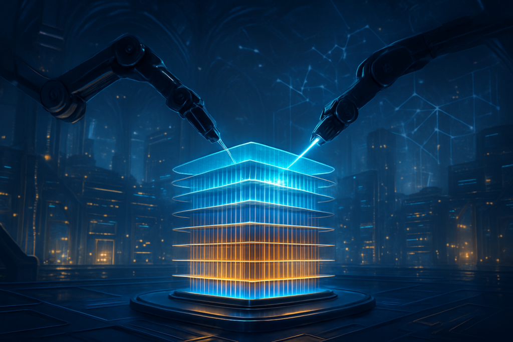
Engineering the Future: P&T7 and the HBM4 Revolution
The technical centerpiece of the $13 billion strategy is the integration of the P&T7 facility with the existing M15X DRAM fab. This geographical proximity allows for a seamless "wafer-to-package" flow, significantly reducing the risks of damage and contamination during transit while boosting overall production yields. Unlike previous generations of memory, HBM4 features a 16-layer stack—revealed at CES 2026 with a massive 48GB capacity—which demands extreme thinning of silicon wafers to just 30 micrometers.
To achieve this, SK Hynix is doubling down on its proprietary Advanced Mass Reflow Molded Underfill (MR-MUF) technology, while simultaneously preparing for a transition to "Hybrid Bonding" for the subsequent HBM4E variant. Hybrid Bonding eliminates the traditional solder bumps between layers, using copper-to-copper connections that allow for denser stacking and superior heat dissipation. This shift is critical as next-gen GPUs from Nvidia (NASDAQ: NVDA) and AMD (NASDAQ: AMD) consume more power and generate more heat than ever before. Furthermore, HBM4 marks the first time that the base die of the memory stack will be manufactured using a logic process—largely in collaboration with TSMC (NYSE: TSM)—further blurring the line between memory and processor.
Strategic Realignment: The Packaging Triangle and Market Dominance
The construction of P&T7 completes what SK Hynix executives are calling the "Global Packaging Triangle." This three-hub strategy consists of the Icheon site for R&D and HBM3E, the new Cheongju mega-hub for HBM4 mass production, and a $3.87 billion facility in West Lafayette, Indiana, which focuses on 2.5D packaging to better serve U.S.-based customers. By spreading its advanced packaging capabilities across these strategic locations, SK Hynix is building a resilient supply chain that can withstand geopolitical volatility while remaining close to the Silicon Valley design houses.
For competitors like Samsung Electronics (KRX: 005930) and Micron Technology (NASDAQ: MU), this $13 billion "preemptive strike" raises the stakes significantly. While Samsung has been aggressive in developing its own HBM4 solutions and "turnkey" services, SK Hynix's specialized focus on the packaging process—the "back-end" that has become the "front-end" of AI value—gives it a tactical advantage. Analysts suggest that the ability to scale 16-layer HBM4 production faster than competitors could allow SK Hynix to maintain its current 50%+ market share in the high-end AI memory segment throughout the late 2020s.
The End of Commodity Memory: A New Era for AI
The sheer scale of the SK Hynix investment underscores a fundamental shift in the semiconductor industry: the death of "commodity memory." For decades, DRAM was a cyclical business driven by price fluctuations and oversupply. However, in the AI era, HBM is treated as a bespoke, high-value logic component. This $13 billion strategy highlights how packaging has evolved from a secondary task to the primary driver of performance gains. The ability to stack 16 layers of high-speed memory and connect them directly to a GPU via TSMC’s CoWoS (Chip-on-Wafer-on-Substrate) technology is now the defining challenge of AI hardware.
This development also reflects a broader trend of "logic-memory fusion." As AI models grow to trillions of parameters, the "memory wall"—the speed gap between the processor and the data—has become the industry's biggest hurdle. By investing in specialized hubs to solve this through advanced stacking, SK Hynix is not just building a factory; it is building a bridge to the next generation of generative AI. This aligns with the industry's movement toward more specialized, application-specific integrated circuits (ASICs) where memory and logic are co-designed from the ground up.
Looking Ahead: Scaling to HBM4E and Beyond
Construction of the P&T7 facility is slated to begin in April 2026, with full-scale operations expected by 2028. In the near term, the industry will be watching for the first certified samples of 16-layer HBM4 to ship to major AI lab partners. The long-term roadmap includes the transition to HBM4E and eventually HBM5, where 20-layer and 24-layer stacks are already being theorized. These future iterations will likely require even more exotic materials and cooling solutions, making the R&D capabilities of the Cheongju and Indiana hubs paramount.
However, challenges remain. The industry faces a global shortage of specialized packaging engineers, and the logistical complexity of managing a "Packaging Triangle" across two continents is immense. Furthermore, any delays in the construction of the Indiana facility—which has faced minor regulatory and labor hurdles—could put more pressure on the South Korean hubs to meet the voracious appetite of the AI market. Experts predict that the success of this strategy will depend heavily on the continued tightness of the SK Hynix-TSMC-Nvidia alliance.
A New Benchmark in the Silicon Race
SK Hynix’s $13 billion commitment is more than just a capital expenditure; it is a declaration of intent in the race for AI supremacy. By building the world’s largest and most advanced packaging hub, the company is positioning itself as the indispensable foundation of the AI revolution. The move recognizes that the future of computing is no longer just about who can make the smallest transistor, but who can stack and connect those transistors most efficiently.
As P&T7 breaks ground in April, the semiconductor world will be watching closely. The project represents a significant milestone in AI history, marking the point where advanced packaging became as central to the tech economy as the chips themselves. For investors and tech giants alike, the message is clear: the road to the next breakthrough in AI runs directly through the specialized packaging hubs of South Korea.
This content is intended for informational purposes only and represents analysis of current AI developments.
TokenRing AI delivers enterprise-grade solutions for multi-agent AI workflow orchestration, AI-powered development tools, and seamless remote collaboration platforms.
For more information, visit https://www.tokenring.ai/.