As of January 2026, the semiconductor industry has officially entered what historians may one day call the "Glass Age." For decades, the foundation of chip packaging relied on organic resins, but the relentless pursuit of artificial intelligence has pushed these materials to their physical breaking point. With the latest generation of AI accelerators now demanding upwards of 1,000 watts of power, industry titans like Intel and Samsung have pivoted to glass substrates—a revolutionary shift that promises to solve the thermal and structural crises currently bottlenecking the world’s most powerful hardware.
The transition is more than a mere material swap; it is a fundamental architectural redesign of how chips are built. By replacing traditional organic substrates with glass, manufacturers are overcoming the "warpage wall" that has plagued large-scale multi-die packages. This development is essential for the rollout of next-generation AI platforms, such as NVIDIA’s recently announced Rubin architecture, which requires the unprecedented stability and interconnect density that only glass can provide to manage its massive compute and memory footprint.
Engineering the Transparent Revolution: TGVs and the Warpage Wall
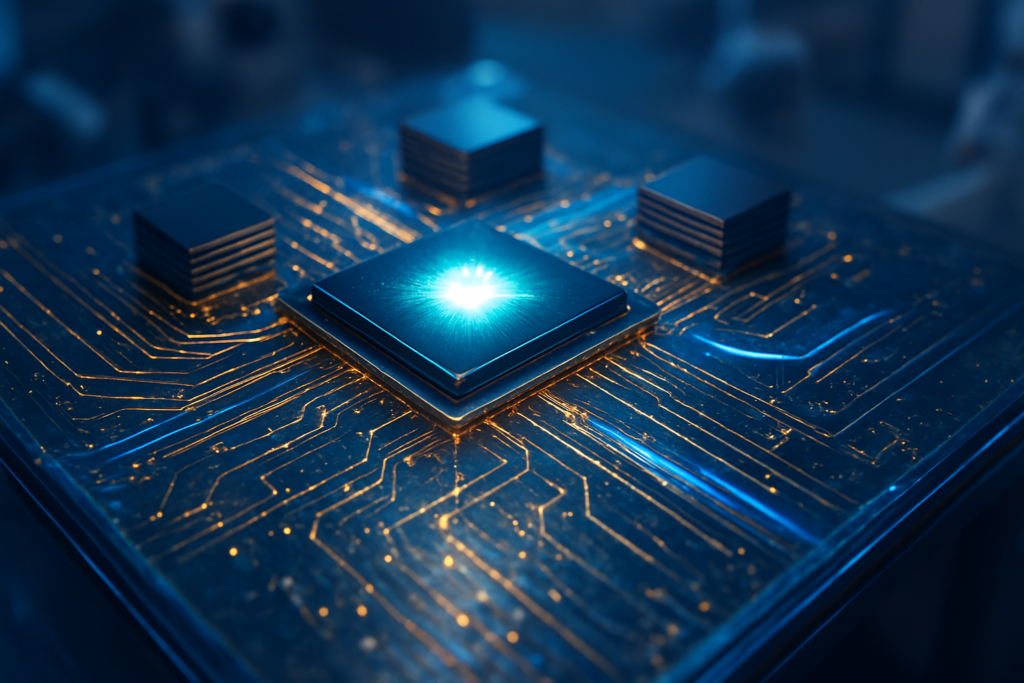
The technical shift to glass is necessitated by the extreme heat and physical size of modern AI "super-chips." Traditional organic substrates, typically made of Ajinomoto Build-up Film (ABF), have a high Coefficient of Thermal Expansion (CTE) that differs significantly from the silicon chips they support. As a 1,000-watt AI chip heats up, the organic substrate expands at a different rate than the silicon, causing the package to bend—a phenomenon known as the "warpage wall." Glass, however, can have its CTE precisely tuned to match silicon, reducing structural warpage by an estimated 70%. This allows for the creation of massive, ultra-flat packages exceeding 100mm x 100mm, which were previously impossible to manufacture with high yields.
Beyond structural integrity, glass offers superior electrical properties. Through-Glass Vias (TGVs) are laser-etched into the substrate rather than mechanically drilled, allowing for a tenfold increase in routing density. This enables pitches of less than 10μm, allowing for significantly more data lanes between the GPU and its memory. Furthermore, glass's dielectric properties reduce signal transmission loss at high frequencies (10GHz+) by over 50%. This improved signal integrity means that data movement within the package consumes roughly half the power of traditional methods, a critical efficiency gain for data centers struggling with skyrocketing electricity demands.
The industry is also moving away from circular 300mm wafers toward large 600mm x 600mm rectangular glass panels. This "Rectangular Revolution" increases area utilization from 57% to over 80%. By processing more chips simultaneously on a larger surface area, manufacturers can significantly increase throughput, helping to alleviate the global shortage of high-end AI silicon. Initial reactions from the research community suggest that glass substrates are the single most important advancement in semiconductor packaging since the introduction of CoWoS (Chip-on-Wafer-on-Substrate) nearly a decade ago.
The Competitive Landscape: Intel’s Lead and Samsung’s Triple Alliance
Intel Corporation (NASDAQ: INTC) has secured a significant first-mover advantage in this space. Following a billion-dollar investment in its Chandler, Arizona, facility, Intel is now in high-volume manufacturing (HVM) for glass substrates. At CES 2026, the company showcased its 18A (2nm-class) process node integrated with glass cores, powering the new Xeon 6+ "Clearwater Forest" server processors. By successfully commercializing glass substrates ahead of its rivals, Intel has positioned its Foundry Services as the premier destination for AI chip designers who need to package the world's most complex multi-die systems.
Samsung Electronics (KRX: 005930) has responded with its "Triple Alliance" strategy, integrating its Electronics, Display, and Electro-Mechanics (SEMCO) divisions to fast-track its own glass substrate roadmap. By leveraging its world-class expertise in display glass, Samsung has brought a high-volume pilot line in Sejong, South Korea, into full operation as of early 2026. Samsung is specifically targeting the integration of HBM4 (High Bandwidth Memory) with glass interposers, aiming to provide a thermal solution for the memory-intensive needs of NVIDIA (NASDAQ: NVDA) and Advanced Micro Devices (NASDAQ: AMD).
This shift creates a new competitive frontier for major AI labs and tech giants. Companies like NVIDIA and AMD are no longer just competing on transistor density; they are competing on packaging sophistication. NVIDIA's Rubin architecture, which entered production in early 2026, relies heavily on glass to maintain the integrity of its massive HBM4 arrays. Meanwhile, AMD has reportedly secured a deal with Absolics, a subsidiary of SKC (KRX: 011790), to utilize their Georgia-based glass substrate facility for the Instinct MI400 series. For these companies, glass substrates are not just an upgrade—they are the only way to keep the performance gains of "Moore’s Law 2.0" alive.
A Wider Significance: Overcoming the Memory Wall and Optical Integration
The adoption of glass substrates represents a pivotal moment in the broader AI landscape, signaling a move toward more integrated and efficient computing architectures. For years, the "memory wall"—the bottleneck caused by the slow transfer of data between processors and memory—has limited AI performance. Glass substrates enable much tighter integration of memory stacks, effectively doubling the bandwidth available to Large Language Models (LLMs). This allows for the training of even larger models with trillions of parameters, which were previously constrained by the physical limits of organic packaging.
Furthermore, the transparency and flatness of glass open the door to Co-Packaged Optics (CPO). Unlike opaque organic materials, glass allows for the direct integration of optical interconnects within the chip package. This means that instead of using copper wires to move data, which generates heat and loses signal over distance, chips can use light. Experts believe this will eventually lead to a 50-90% reduction in the energy required for data movement, addressing one of the most significant environmental concerns regarding the growth of AI data centers.
This milestone is comparable to the industry's shift from aluminum to copper interconnects in the late 1990s. It is a fundamental change in the "DNA" of the computer chip. However, the transition is not without its challenges. The current cost of glass substrates remains three to five times higher than organic alternatives, and the fragility of glass during the manufacturing process requires entirely new handling equipment. Despite these hurdles, the performance necessity of 1,000-watt chips has made the "Glass Age" an inevitability rather than an option.
The Horizon: HBM4 and the Path to 2030
Looking ahead, the next two to three years will see glass substrates move from high-end AI accelerators into more mainstream high-performance computing (HPC) and eventually premium consumer electronics. By 2027, it is expected that HBM4 will be the standard memory paired with glass-based packages, providing the massive throughput required for real-time generative video and complex scientific simulations. As manufacturing processes mature and yields improve, analysts predict that the cost premium of glass will drop by 40-60% by the end of the decade, making it the standard for all data center silicon.
The long-term potential for optical computing remains the most exciting frontier. With glass substrates as the foundation, we may see the first truly hybrid electronic-photonic processors by 2030. These chips would use electricity for logic and light for communication, potentially breaking the power-law constraints that have slowed the advancement of traditional silicon. The primary challenge remains the development of standardized "glass-ready" design tools for chip architects, a task currently being tackled by major EDA (Electronic Design Automation) firms.
Conclusion: A New Foundation for Intelligence
The shift to glass substrates marks the end of the organic era and the beginning of a more resilient, efficient, and dense future for semiconductor packaging. By solving the critical issues of thermal expansion and signal loss, Intel, Samsung, and their partners have cleared the path for the 1,000-watt chips that will power the next decade of AI breakthroughs. This development is a testament to the industry's ability to innovate its way out of physical constraints, ensuring that the hardware can keep pace with the exponential growth of AI software.
As we move through 2026, the industry will be watching the ramp-up of Intel’s 18A production and Samsung’s HBM4 integration closely. The success of these programs will determine the pace at which the next generation of AI models can be deployed. While the "Glass Age" is still in its early stages, its significance in AI history is already clear: it is the foundation upon which the future of artificial intelligence will be built.
This content is intended for informational purposes only and represents analysis of current AI developments.
TokenRing AI delivers enterprise-grade solutions for multi-agent AI workflow orchestration, AI-powered development tools, and seamless remote collaboration platforms.
For more information, visit https://www.tokenring.ai/.